Induction Balance Metal Detector
The following report is written by Andrei Chtchedrine of Russia. It describes a pretty complex induction balance detector. His HTML page (English version) is reproduced here with his permission - you can view the original at his web site ( www.aha.ru/~aish/indexe.htm) or the Russian version at www.aha.ru/~aish/index.html. Questions are best directed at Andrei, but I will attempt to answer questions posted to Geotech as well. Thanks Andrei!
6.3 One coil induction metal detector
Offered induction type metal detector is all-purpose. Its sensor is simple in construction and can be made with 0,1-1(m) diameter. The size of discovered targets and distance of discovering of these targets will be changed ratable to its dimensions. The depth of discovering for standard sensor with diameter 180 (mm) is:
- coin Æ 25 (mm) - 0,15 (m)
- pistol - 0,4 (m)
- helmet - 0,6 (m)
Device is provided with the simplest discriminator which enables to select the signals coming from small iron objects if they are of no particular importance for seeking.
Functional diagram
Functional diagram is performed in feature 25. It consists of some functional blocks. Quartz oscillator is a source of square wave pulses from which in prospect the signal, going to the coil of sensor, is formed. Oscillator signal is quartered by frequency with ring counter on the flip-flops. Counter is done at mesh circuit in order to have possibility to form two signals F1 and F2 at its outputs, dislocated in relation to each other at (90o) phase shift that is necessary condition for discriminator constructing.
Feature 25. Induction metal detector functional diagram.
Square wave signal (meander) is approached to input of the first integrator and when it comes out it turns into piecewise-smooth "sawtooth" voltage. The second integrator forms the signal which is close to sinusoidal one and consists of half-waves of parabolic shape. This stability amplitude signal comes to power amplifier which is voltage-to-current converter loaded onto sensor coil. Voltage of sensor isn't stable any longer by amplitude as it depends on signal reflected from metal targets. Absolute value of this instability is greatly little. To enhance it scilicet to isolate friendly signal there is second integrator output voltage deduction from sensor coil voltage in compensation circuit.
|
|
In this text a lot of details of power amplifier constructing, compensation circuit and the way of switching on the sensor coil are counted out knowingly in order to make this description easier for understanding of device basic principles, in spite of being partly incorrect. To get more details see the description of circuit diagram . |
From the compensation circuit friendly signal comes into input amplifier where its voltage gain happens. Synchronous detectors convert friendly signal into slow changing voltages whose value and polarity depend on shift of phase reflected signal in relation to voltage signal of sensor coil.
Hereby output signals of synchronous detectors are nothing else than the components of vector orthogonal resolution of friendly reflected signal at basis of fundamental harmonics (i.e. first overtones) of reference signals F1 and F2.
A part of useless signal, which is uncompensated with compensation circuit because of its imperfection, inevitably penetrates into input amplifier. This part of signal converts into direct current voltage at the outputs of synchronous detectors. High-pass filters (HPF) cut off useless direct components passing and enhancing only changing signal components which are connected with the sensor movement in relation to metal subjects. Discriminator issues control signal to run audio tone former only if there is determinate combination of signal polarity at filters' output so sound indication from petty piddling iron things, rust and some minerals is excluded.
Schematic diagram
Schematic diagram of induction metal detector is performed in feature 26 - its input part, feature 27 - synchronous detectors and filters, feature 28 - discriminator and audio tone former, feature 29 - general connection diagram.
Quartz oscillator (feat. 26)
Quartz oscillator is built with inverters D1.1-D1.3. Frequency of oscillator is stabilized with quarts or piezoelectric ceramic resonator Q with resonance frequency 215 (Hz) » 32 (kHz) ("clock quartz"). Circuit R1C2 blocks free-running of oscillator on high overtones. Circuit NFL (negative feedback loop) is closed with resistor R2, and with resonator Q - circuit PFL (positive feedback loop). Oscillator is distinguished by simplicity, little power consumption, works error-free at power supply voltage 3-15 (V), does not contain trimming elements and too high-value (megohms) resistors. Oscillator output frequency is about 32 (kHz).

Feat.26. Induction metal-detector electrical schematic diagram.
Input circuits.
Ring counter (feat. 26)
Ring counter fulfills two functions. Firstly it quarters oscillator frequency in order to get 8(kHz) (to chose frequencies go to chapter 1.1. for recommendations). Secondly it forms two reference signals for synchronous detectors dislocated 90o phase shift in relation to each other.
Ring counter is presented with two D-triggers D2.1 and D2.2, closed into ring with signal inversion along the ring. Clock signal is mutual for both of triggers. Any output signal of first trigger D2.1 has +90o or -90o phase shift in relation to any output signal of second trigger D2.2.
Integrators (feat. 26)
They are fabricated on OA (operational amplifiers) D3.1 and D3.2. Their time constants are determined by circuits R3C6 and R5C9. Regime to direct current voltage is suspended with resistors R4, R6. Isolating condensers C5, C8 interfere with static error storing, which can break integrators from regime because of their great direct current voltage amplification. Element values are chosen so that the summarized phase shift both of integrators at output frequency 8 (kHz) will amount 180o exactly with allowance as basic main capital RC-circuits as with allowance for influence of crossover circuits and limited OA speed for chosen correction. OA correction circuits of integrators are conventional and consist of 33 (pF) capacitors.
Power amplifier (feat.26)
It is fabricated on OA D4.2 with parallel voltage negative feedback. Temperature compensated current-carrying shunt which consists of resistors R71, R72 and temperature sensitive resistor or thermistor R73 (go to feat.29) is placed between output of second integrator and inverting input of OA D4.2. The power amplifier load which is a component of feedback loop element at the same time appears as oscillator circuit LC consisting of sensor coil L1 and capacitor C61.
|
|
In diagrams shown in features 26-29 some positions are missed in numeration of resistors and capacitors. It is connected with multiple modifications of induction metal detector schematic diagram and is not an error. |
Oscillating circuit is adjusted to resonance at quarter of frequency of quartz resonator of master oscillator, scilicet to frequency of incoming signal. Impedance modulus of oscillating circuit at resonance frequency amounts about 4 (kOhm). Characteristics of sensor coil L1 are:
winding number - 100,
copper wire diameter being 0,3-0,5 (mm),
medium diameter and diameter of fixture for winding is 165 (mm).
The coil has got a shield made of alfol, connected to common wire of device. To prevent from short-circuit winding formed by alfol shield, small part of coil winding circle perimeter about 1 (cm) is free from the shield.
Sensor components R71 - R73 and L1, C61 are gathered so that, firstly, they would be amounted at voltage value at input and output of power amplifier. To get that it is necessary: curtain resistance R71 -R73 would be amounted to impedance modulus of oscillating circuit L1, C61 at resonance frequency 8 (kHz), more true 8192 (Hz). This resistance module amounts about 4 (kOhm) and its magnitude should be specified for concrete sensor. Secondly, resistance temperature coefficient (TCR) of circuit R71 - R73 must coincide in quantity and in sign with TCR of impedance modulus of oscillating circuit L1, C61 at resonance frequency, what is achieved rough - just with choosing the thermistor rating R73, more accurate - with choosing correlation R71 - R72, it's achieved tentatively in tuning.
|
|
Oscillating circuit temperature instability is connected, first of all, with instability of sensor coil copper wire resistance. As the temperature is rising up this resistance is rising up too and the losses at circuit are enhanced so its Q-factor is degraded. Thus, impedance modulus at resonance frequency is getting diminished. |
Resister R18 doesn't mean much and is destined for suspending OA D4.2 in mode if connector coupler X1 is turned off. OA correction circuit D4.2 is conventional and consists of 33 (pF) capacitor.
Compensation circuit (Feat. 26)
Its main elements which realize subtraction of second integrator output voltage from sensor coil voltage - are resistors R15, R17 with equal impedance value. Friendly signal comes into input amplifier from their mutual connecting point. Additional elements used for manual tuning and fine tuning of device are potentiometers R74, R75 (feat. 29). These potentiometers allow to take signal being at interval [ - 1, + 1] from the signal of sensor voltage (or practically the one which is equal to second integrator output signal at amplitude). Minimal signal at input amplifier and null signals at synchronous detectors outputs are achieved with these potentiometers tuning.
A part of one potentiometer output signal is admixed into compensation circuit with resistor R16 directly, and with elements R11-R14, C14-C16 with 90 o shift from another output potentiometer.
OA D4.1 is the basic of the highest harmonic compensation circuit compensator. Double integrator with inversion is fulfilled on it; time constant of this double integrator is controlled by common for integrator circuit which is parallel to NFL at R7C12 voltage, and also by capacitor C16 with all resistors which surround it. 8 (kHz) frequency square wave pulse comes into double integrator input from the element output D1.5. First overtone signal is deducted from square wave pulses with resistors R8, R10. Summarized impedance of these resistors is about 10 (kOhm) and achieved tentatively in tuning by signal minimal value at OA D4.1 output. The highest harmonics, kept at double integrator output, come into compensation circuit at the same amplitude as the highest harmonics penetrating through the main integrators. Phase correlation is so that the highest harmonics from two these sources are practically compensated.
|
|
Power amplifier output isn't additional source of the highest harmonics, as oscillating circuit high Q-factor (about 30) provides high level of the highest harmonic depressing. As a matter of fact the highest harmonics don't influence on device normal work even though they multiple exceed friendly reflected signal. However they need diminishing so that the input amplifier doesn't happen to be into output voltage limitation mode, when the ups of "mixture" consisted of the highest harmonics get cut off because of limited voltage value of OA power supply. Friendly signal amplification factor Kv gets abruptly degraded with such kind of amplifier transiting into nonlinear mode. Elements D1.4 and D1.5 prevent making extraneous PFL (positive feedback loop) with resistor R7 because of output impedance nonzero value of D2.1 trigger output. Connecting attempt of resistor R7 directly to trigger comes to low frequency free-running oscillations of compensation circuit. |
OA D4.2 correction circuit is conventional and consists of 33 (pF) capacitor.
Input amplifier (Feat. 26)
Input amplifier is two stages. Its first stage is built on OA D5.1 with parallel NFL (negative feedback loop) at voltage. Friendly signal amplification coefficient is KV = - R19/R17 » - 5. The second stage is built on OA D5.2 with serial NFL at voltage. Amplification coefficient is KV = R21/R22 + 1 = 6. Time constants of crossover circuits are chosen so that the phase incursion made of them at operating frequency would compensate signal delay stipulated by final OA response speed. Correction circuits of OA D5.1 and D5.2 are conventional and consist of 33(pF) capacitors.
Synchronous detectors (Feat.27)
Synchronous detectors are similar and have the same diagrams, so only one of them will be examined, the upper one in diagram. Synchronous detector consists of balance modulator, integrating circuit and direct current voltage amplifier (DCVA). Balance modulator is actualized on the base of integrated circuit of field-effect transistor analog switches D6.1. Analog switches at 8 (kHz) frequency connect "triangle" outputs of integrating circuit to global (common) bus. This integrating circuit consists of resistors R23 and R24 and capacitor C23. Base frequency signal comes to balance modulator from one of the outputs of ring counter. This signal is controlling for analog switches.
Integrating circuit input "triangle" signal comes through the crossover capacitor C21 from the output of input amplifier.
Feat.27. Induction metal-detector electrical schematic diagram.
Synchronous detectors and filters.
Integrating circuit time constant is t » R23× C23 = R24× C23.
OA of direct current voltage amplifier (DCVA) D7 has got conventional correction circuit, which consists of 33 (pF) capacitors for OA K140UD1408 type. In case of using OA K140UD12 type (with internal correction), correction capacitor isn't wanted, however auxiliary voltage driving resistor R68 is wanted (shown by dotted line).
Filters (Feat. 27)
Filters are similar and have the same diagrams, so only one of them will be examined, the upper one in diagram.
As stated above, by its type the filter appertains to high-pass filters (HPF). Besides that, its task in circuit is to keep on enhancing synchronous detector rectified signal. There is a specific problem in metal-detector working by using such kind of filters. Here is the essence of it. Friendly signals, which come from synchronous detector outputs are comparatively slow, so HPF cut-off frequency is commonly in 2-10 (Hz) band. Amplitude band width of signals is very large and can reach 60 (dB) at filter input. It means that filter will work at amplitude overload nonlinear mode very often. Linear HPF returning from nonlinear mode after impacting such large amplitude overload may last for score or two of seconds (so is readiness device time after supply switching), this makes common filter designs unsuitable in practice.
To resolve this problem one tries some kind of gimmicks. More often filter is divided into three-four stages with comparatively little amplification factor and quite equal dispatch of timing circuits at stages. Such solution hastens device returning into normal working mode after overloading. But, it demands a lot of OA.
In offered diagram HPF is one-stage. To diminish over-load consequences it is fulfilled nonlinear. Its time constant for large signals is 60 times less than for little amplitude signals.
Circuitry (from the point of view of schematic diagram), HPF performs voltage amplifier at OA D9.1, straddled by NFL circuit with integrator at OA D10. For little signal, HPF frequency and time responses are determined by divider from resistors R45, R47, integrator time constant R43C35 and amplification coefficient of voltage amplifier at OA D9.1. By HPF output voltage enhancing, after some boundary, influence of diode circuit VD1-VD4 begins to dawn; these diodes are the main source of nonlinearity. This circuit at large signals shunts resistor R45, enhancing NFL depth in HPF and diminishing HPF time constant.
Friendly signal amplification coefficient is about 200. There is capacitor C31 in filter diagram to dejam high-frequency interference. OA of voltage amplifier D9.1 has conventional correction circuit, which consists of 33 (pF) capacitor. OA of integrator D10 has correction circuit, which consists of 33 (pF) capacitor for OA K140UD1408 type. In case of using OA K140UD1408 type (with internal correction) correction capacitor isn't wanted, but auxiliary voltage driving resistor R70 is wanted (shown by dotted line).
Feat.28. Induction metal-detector electrical schematic diagram.
Audio tone discriminator and former.
Discriminator (Feat. 28)
Discriminator consists of comparators at OA D12.1, D12.1 and monostable multivibrators at triggers D13.1, D13.2. When metal-detector sensor moves above metal object friendly signal appears at filter outputs as two voltage half-waves with opposite polarity, which follow one after another simultaneously at each output. For little iron objects both filter output signals will be synchronous: output voltage swings first to minus, then to plus and comes back to zero. For nonferromagnetic metals and large iron objects the response will be different: output voltage of only the first (upper filter in diagram) swings first to minus, and then to plus. At the output of second filter reaction will be opposite: output voltage swings first in plus, and then in minus.
Thus, having determined what polarity half-wave at first filter output was the first in time, it is possible to get definition of the found object type. Discriminator taking decision process is happening like that. Comparators D12.1, D12.2 form positive polarity rectangular pulses at their outputs at some boundary modulus overtopping filter output voltage negative half-wave. This boundary is driven by divider R51, R52 and is about 1 (V).
Comparator output impulses run one of monostable multivibrators at triggers D13.1, D13.2. Monostable multivibrators can't be run synchronously - cross feedback with diodes VD9, VD11 blocks monostable multivibrator run if another one has been run. Impulse duration at monostable multivibrator outputs is about 0,5 (sec) and it is some times more than duration of friendly signal both bumps if sensor moves fast. That's why filter output signal second half-waves don't affect at discriminator decision - by the first bumps of friendly signal it runs on of the monostable multivibrators, blocking other one, and such condition is fixed for 0,5 (sec).
To except comparators actuation from interference, and also to delay the first filter output signal in time in relation to the second one, integrating circuits R49, C41 and R50, C42 are placed at comparator inputs. Circuit R49, C41 time constant is a few times more, so when two half-waves from filter outputs come simultaneously, comparator D12.2 will react the first and trigger D13.2 monostable multivibrator will be run, giving out the control signal ("ferro" - iron).
Audio tone former (Feat. 28)
Audio tone former (ATF) consists of two identical audio frequency controlled generators at Schmitt triggers with "And" logic at input D14.1, D14.2. Each generator is run by output signal of according discriminator monostable multivibrator. If the command "metal" - nonferromagnetic target or large iron object - comes from upper monostable multivibrator output, upper generator starts working and giving out 2 (kHz) frequency tone sequence. If the command "ferro" - small iron objects - comes from lower generator starts working and giving out 500 (Hz) frequency tone sequence. Sequences' duration amounts to impulse's duration at monostable multivibrator outputs. Signal mixing of two tone generators is done by element D14.3. Element D14.4, connected as inverter, is destined for realization of piezoelectric horn connecting bridge circuit. Resistor R63 abridges the bumps of integrated circuit D14 consumption current, which are aroused by capacitive impedance of piezoelectric horn. It is prophylactic to diminish influence of power supply circuits interferences and to prevent from possible stages of amplification self-oscillation.
Peripheral connection diagram (Feat. 29)
The elements, not mounted on the printed board of metal detector and connected to it with electrical demountable connectors, are shown in the peripheral connection diagram. They are:
- tuning and balancing potentiometers (resistors) R74, R75
- sensor with cord assembly and demountable connector
- power supply protective diodes VD13, VD14
- mode switches S1.1-S1.6
- microampermeters W1, W2
- supply buttery
- piezoelectric horn Y1.
Destination of named elements, in general, doesn't desire additional illustrations.
Feat.29. Induction metal-detector electrical schematic diagram.
Peripheral connection diagram.
Types of details and architecture
The types of used integrated circuits are given in table.
Table.
|
Designation feat.26 - feat.28 |
Type |
Functional description (legend) |
|
D1 D2, D13 D3-D5, D9, D12 D6 D7-D8, D10-D11 D14 |
K561LN2 K561TM2 K157UD2 KR590KN4 KR140UD1408 K561TL1 |
6 inverters 2 D-triggers 2 OA's analog switches instrumental OA 4 elements 2AND-NOT with Schmitt triggers at inputs |
Instead of series K561 integrated circuits it is possible to use series K1561 (or CMOS integrated circuits of world-wide 40XX and 40XXX series).
K157 series duplex OA may be changed by any parameter similarity single OA of general purposes (with according changes in pins numbering and correction circuits), though duplex OA application is much more easy-to-use (circuit density is increasing). It is advisable, OA applied types don't be inferior in speed to recommended types. Especially it concerns of D3-D5 integrated circuits.
OA of synchronous detectors and HPF integrators in their parameters must approximate to instrumental OA. Besides the type, named in table, K140UD14, 140UD14, (LM108) are suitable. It is possible to apply ultra-low-consumption OA K140UD12, 140UD12, KR140UD1208, (MC1776) in fit connection circuit.
As to resistors, applied in metal-detector circuit, they aren't put in special requests. They should barely have rugged and diminutive structure and be easy-to-use for building. On purpose to get total temperature stability it's recommended to apply only metal-film resistors in sensor circuits, integrator circuits and in compensation circuit. Value of dissipated power is 0,125-0,25 (W).
Heat-variable resistor (or thermistor) R73 should have negative temperature coefficient of resistance (TCR) and about 4,7 (kOhm) value.
Compensation potentiometers R74, R75 are recommended being multiturn SP5-44 type or with vernier tuning SP5-35 type. Common potentiometers of any type are suitable too. In this case it had better use two of them. One of them is for rough tuning 10 (kOhm) value, connected as the circuit is supposed. Another one is for fine tuning 0,5-1 (kOhm) value, connected into one of main potentiometer edge output interruption as rheostat circuit is supposed.
Capacitors C45, C49, C51 are electrolytic. Recommended types are K50-29, K50-35, K53-1, K53-4 and other mini dimensions. The rest capacitors, except for capacitors of sensor oscillating circuit, are ceramic K10-7 type (no more than 68 (nF) value) and metal-film K73-17 (more than 68 (nF) value).
Circuit capacitor C61 is special. It is put in special requests about accuracy and temperature stability. Capacitor C61 consists of several (5...10) capacitors, connected in parallel. Resonance circuit tuning is done by selecting capacitor quantity and value. Recommended type of capacitors is K10-43. Capacitors with temperature capacitance factor (TCF) no more than 10-6/K are recommendable. Other types of precision capacitors are also possible to apply, for instance K71-7.
Diodes VD1-VD12 KD521, KD522 types are applied or analogous silicon one of low power. As VD1-VD4 and VD5-VD8 diodes are also easy to use integral diode bridges KD906 type. Pins (+) and (-) of diode bridges are connected together, and with the pins (~) it is connected in circuit instead of four diodes. Protective diodes VD13-VD14 of KD226, KD243, KD247 types and other mini dimension ones are possible to apply with up to 1(A) maximum current.
Microampermeters of any type are connected at 100 (mkA) current with central zero. Mini dimension microampermeters, for instance M4247 type, are easy-to-use.
As quarts resonator Q can be used any small size clock quartz (analogous quarts resonators are also used in potable electronic games).
As mode switch can be used any on 5 positions and on 6 directions mini dimension turn one. Supply batteries are 3R12 type - 2 pcs. on 4,5 (V).
Piezoelectric horn Y1 can be ZP1....ZP18 type.
Demountable connectors are conventional, with 2,5 (mm) pin step (soldering is supposed). Nowadays such kinds of demountable connectors are wide used in TVs and in other consumer technique. Demountable connector X4 should be external with metal external details , it's advisable to have them with silver- or gold-plated contacts and hermetic output to cord. Recommended types are RS7 or RS10 with threaded or bayonet connection.
Printed board
The device construction can be arbitrary enough. The main elements of device schematic diagram are placed on the printed board.
Printed board of metal detector electronic part can be done on the base of completed general-purpose prototyping printed board for integrated circuit with 2,5 (mm) pin distance. In this case bonding is done with monoconductor tinned copper in insulation. Such construction is easy to use in practice.
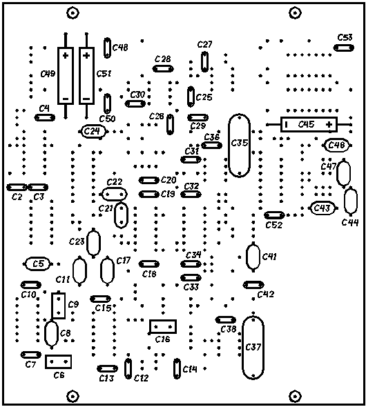
Printed board construction will be more shipshape and trouble-free if the printed wires are traced conventionally. Considering its complexity, in this case printed board should have two-side metal deposition. Topology of printed wires, applied by author, is shown in feature 30 - component setting side printed board image, and in feature 31 - soldering side printed board image. Topology picture isn't given as actual size. To make photocopy fabricating easier, printed board size at external frame of picture is 130 x 144 (mm).
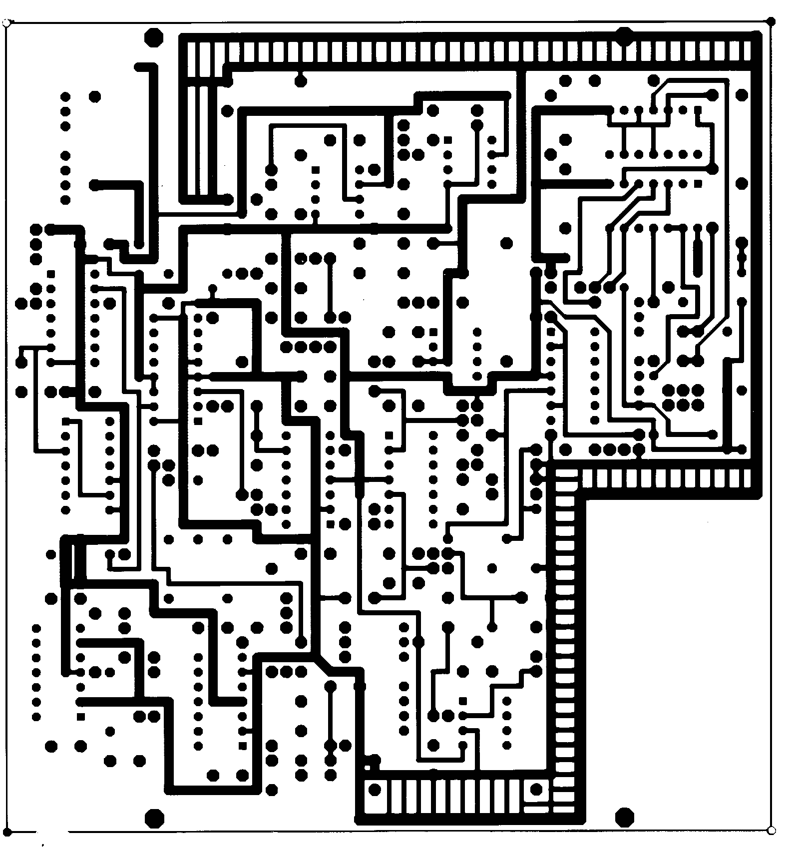
Feat.30. Topology of printed board wires.
Component setting side printed board image.
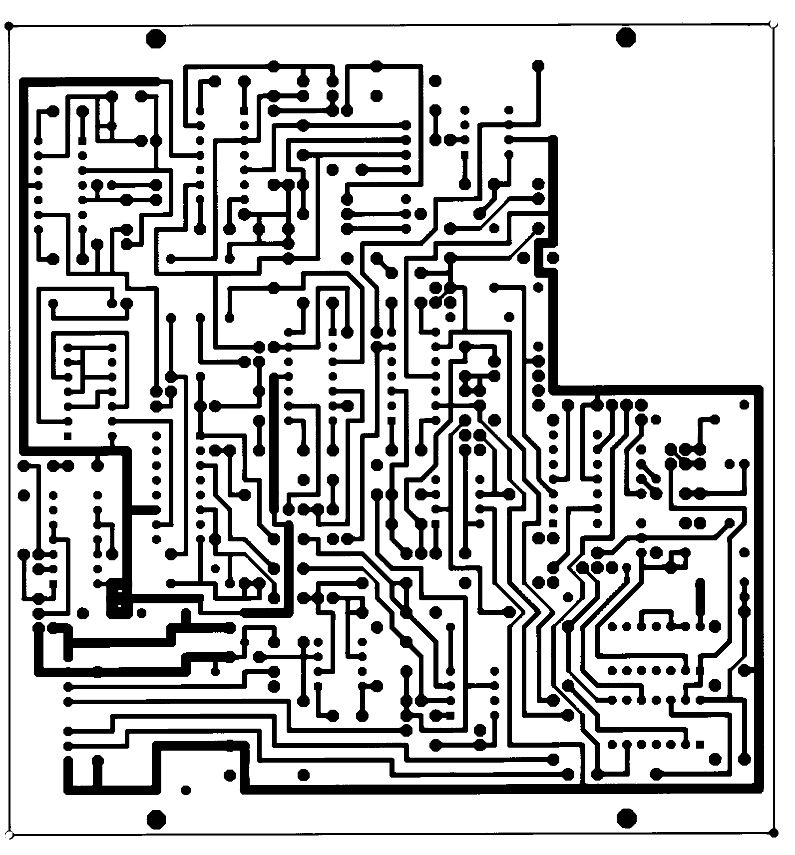
Feat.30. Topology of printed board wires.
Soldering side printed board image.
Printed board specialities.
- wire bridges, without which the printed board tracing is impossible,
- global (common) bus, which is done as straining pattern with maximum square on the board,
- eye configuration in mesh nodes with 2,5 (mm) pin, - minimum distance between the eye center and conductor median or between two neighbour conductor medians is 1,77 (mm),
- conductors wiring direction of printed board is in 45o order.
Component configuration on the printed board is shown in feature 32 (integrated circuits, demountable connectors, diodes and quarts resonator), in feature 33 ( resistors and bridges) and in feature 34 (capacitors).
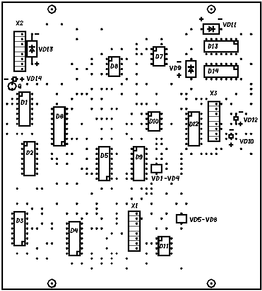
Feat. 32 Component configuration on the printed board.
Demountable connectors, integrated circuits,
diodes and quarts resonator.
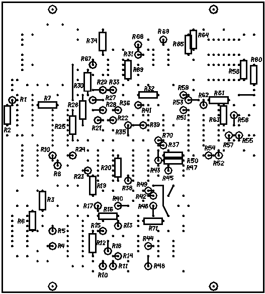
Feat. 33. Component configuration on the printed board. Resistors.
Feat. 34. Component configuration on the printed board. Capacitors.
Device adjusting
Here are some recommendations how to adjust this device in a proper way and following the next order.
- Check building fidelity according to schematic diagram. Sure about short-circuit failure absence between neighbour conductors of printed board, neighbour pins of integrated circuits, and so on.
- Connect supply battery or double-polar feed element, keeping up the polarity exactly. Turn the device on and measure consumption current. It is to be about 40 (mA) for each voltage distribution bus. Severe departure from measured value testifies to incorrect building or integrated circuit defect.
- Make sure that there is about 32 (kHz) frequency fine meander at generator output.
- Make sure that there is about 8 (kHz) frequency meander at outputs of triggers D2.
- Make sure that there is sawtooth voltage at the first integrator output, and practically sinusoidal voltage with zero averages at the second output integrator.
- Make sure in power amplifier working capacity. It is so, if there is 8 (kHz) frequency sinusoidal voltage with zero average at its output (sensor is connected).
- Tune sensor oscillating circuit into resonance with selecting number of oscillating circuit capacitors and their value. Adjustment control is made grossly - over maximum amplitude of circuit voltage, fine adjustment - over 180o phase shift between input and output voltages of power amplifier.
- Replace sensor resistor element (resistors R71-R73) by constant resistor. Select its value so that input and output voltages of power amplifier are equal in amplitude.
- Make sure in input amplifier working capacity. To do it, check up its OA mode and signal propagation.
- Make sure in high overtone compensation circuit working capacity. Obtain minimum of fundamental harmonic signal at input amplifier output with adjustment potentiometers R74, R75. Obtain minimum of high overtones at input amplifier output with selecting additional resistor R8. There is possible some kind of offset in fundamental harmonic. Make it away doing adjustment with potentiometers R74, R75 and regain minimum of high overtones with selecting resistor R8 doing it a few times.
- Make sure in synchronous detectors working capacity. If sensor and compensation circuit are adjusted correctly, synchronous detector output voltages are unset "0" approximately in midposition of potentiometer sliders R74, R75. If it doesn't happen (no errors in construction), it is necessary to tune sensor circuit finer and select its resistor element. Final adjustment sensor validation criterion is device balancing (scilicet "0" setting at synchronous detector outputs) in midposition of potentiometer sliders R74, R75. Tuning the device, make sure that when it is about to be balanced only device W1 responds to knob running of potentiometer R74, and only device W2 responds to knob running of potentiometer R75. If knob running one of the potentiometers, when sensor is about to be balanced, reflects on both of devices synchronously, then, such situation either must be accepted (in this case every time there could be some trouble with balancing when the sensor is switched on), or select finer capacitor R14 value.
- Make sure in filters working capacity. Zero-frequency component at their outputs aren't to be over 100 (mV). If it is so, capacitors C35, C37 should be changed (there could be discarded capacitors even among film capacitors. Use capacitors of less leakege current). There might be necessity of changing OA D10 and D11. Make sure that filters respond to friendly signal, that can be imitated by wheeling knobs R74, R75 imponderably. Movable-pointer indicators W1 and W2 enable to watch filter output signal. Make sure that filter output voltage is reset "0" after large amplitude signal influence ( no later than 2 (sec)).
- Make sure in discriminator and audio-tone forming circuit working capacity.
- Execute stress relief heat treatment of sensor. To do it firstly metal detector needs tuning and balancing taking resistor instead of sensor resistive element. Then, heat the sensor up a little and cool it down. Fix in what position of potentiometer slider "metal" R74 device balance will be achieved under changed sensor temperature. Measure resistor resistance, installed into sensor temporally, and replaced it by R71-R73 circuit with thermistor and resistors such values that R71-R73 circuit summarized resistance would be amounted to replaced constant resistor resistance. Keep the sensor under indoor temperature no less than half an hour and repeat the experiment with temperature changing. Compare found data. If balance positions in slider scale R74 (for these two experiments) shift to the same side (look to each other), it means that sensor is undercompensated and thermistor influence needs increasing, having diminished resistor R72 shunting influence, for that enhance its resistance, and diminish the additional resistor R71 resistance (to keep the whole circuit resistance value constant). If balance positions for these two experiments shift to opposite sides, it means that sensor is overcompensated and thermistor influence needs diminishing, having enhanced resistor R72 shunting influence, for that diminish its resistance and enhance the additional resistor R71 resistance (to keep the whole circuit resistance value constant). Having done e few experiments on selecting of resistors R71 and R72, it is necessary to achieve that tuned and balanced device doesn't lose its ability to be balanced if temperature has 40oK changing (cooling from indoor temperature to freezing room temperature).
Attention! Further device tuning is required to fulfill far from large metal things, including measurement instrumentation! Otherwise, the device can got upset if it moves close to them. The adjustment will be impossible in any case if there are large metal objects near sensor.
|
|
It might occur that adverse electromagnetic environment will encumber device tuning. In this case meter needles of microampermeters will commit chaotic or periodic oscillation if device is tuned into switch position S1 "Mode 1" and "Mode 2". This described appearance is unwanted and can be explained by interferences of 50-60 (Hz) domestic electrical power net high overtones with sensor coil. If device is tuned and moved away from cable under electric tension, meter needle oscillation is to be out. |
If there are some faults and departures of some units in working of metal detector circuit act as it is accepted:
- check OA self-oscillation absence,
- check OA modes by direct current,
- signals and input/output logical levels of digital ICs (integrated circuits)
- and so on.